Difference between revisions of "Camera Sensor Basics"
(→Link Basics) |
(→I/O Signaling) |
||
| Line 50: | Line 50: | ||
'''Note: In normal operation, data lanes are constantly switching between low-power control mode and high-speed data transfer mode.''' | '''Note: In normal operation, data lanes are constantly switching between low-power control mode and high-speed data transfer mode.''' | ||
| − | [[File: Lane states description.png|900px|thumb|center|Table that shows the Lane state descriptions. Taken from i.MX8 RT MIPI DSI and CSI 2 documentation]] | + | [[File: Lane states description.png|900px|thumb|center|Table that shows the Lane state descriptions. Taken from i.MX8 RT MIPI DSI and CSI 2 documentation.]] |
== DDR clocking == | == DDR clocking == | ||
Revision as of 18:37, 14 March 2023
Contents
Overview
This wiki describes relevant concepts when dealing with camera sensors. It represents a useful handbook especially when becomes to developing a driver for camera sensors. The concepts explained here are not attached to any specific sensor or custom hardware board setup, but you can extrapolate the information presented to apply it based on your needs.
MIPI
The Mobile Industry Processor Interface (MIPI) alliance was founded in 2003 by Arm, Nokia ST, and Texas Instruments. Today there are over 300 members. The focus of the organization is to design and promote hardware and software interfaces that simplify the integration of components built into a device.
- Camera Serial Interface 2 (CSI-2): This specification defines a standard data transmission and the control interface between a peripheral device (like a camera) and a host processor. The specification is focused on the protocols for transferring image data (both still images and video) and basic image sensor control through the Camera Control Interface (CCI). This specification represents a low-level layer in the overall system. It's important to mention that this specification does not cover any advanced imaging system features, like the ones provided by an ISP unit.
- Display Serial Interface (DSI): Specification that defines the data transfer protocol and the interface between a host processor and a peripheral device (in this case a display). As the CSI-2, this specification represents a low-level layer in the overall system.
- D-PHY: Defines the transmission medium (electrical conductors), the input/output circuitry, and the clocking mechanism that captures ones and zeroes from the serial bit stream.
Note: Unlike some hot-pluggable or plug-and-play high-speed interfaces (such as HDMI or USB), the MIPI DSI/CSI-2 interfaces are meant for a fixed and permanent connection in a final design.
D-PHY
D-PHY is the source-synchronous physical layer used by CSI-2 and DSI protocols for physical and electrical communication. The D in D-PHY comes from the Roman numeral for 500. Version 1.0 of the D-PHY specification was written assuming a single lane would communicate on the order of 500 Mbps, and so the D-PHY name was born. In the most recent version of the specification, the actual maximum bit rate per lane is up to 9 Gbps.
Link Basics
- Line: An interconnect or wire or trace between a single pin on a host processor and a pin on a peripheral device.
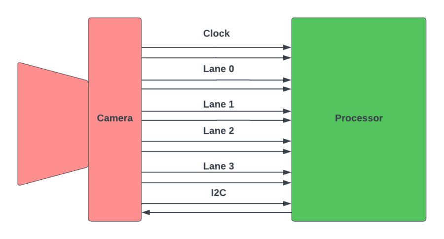
- Lane: Two lines are required to support differential signaling. D-PHY uses a differential pair for high-speed data and clock transmission. This differential pair is referred to as a Lane Interconnect, but mostly shortened to Lane in technical documents.
- Link: A connection between two devices containing one Clock Lane and at least one Data Lane. Many data sheets abbreviate the Link information and/or omit the Link term entirely.
Modes of Operation
There are four modes of operation:
- Control
- High-Speed
- Escape
- Ultra-Low Power State (ULPS)
Data Lanes support all four modes, but Clock Lanes only support Control, High-Speed, and ULPS mode. During normal operation, a Data Lane is in Control or High-Speed mode. High-Speed data transmission happens in bursts and starts from and ends at a Stop state (usually referred to as an LP-11 state), which is in Control mode. The Lane is only in High-Speed mode during data bursts.
I/O Signaling
The D-PHY IO pins have two different electrical modes of operation: single-ended and differential.
- The single-ended mode is referred to as Low Power(LP) mode. It is used during escape and control modes for system configuration/control between the host processor and the peripheral device. In LP mode, the IO circuits use a traditional CMOS output buffer (with slew rate control) that switches between ground and VDD_IO. In LP mode, the two IO circuits, which comprise a lane, can switch independently. They provide four different lane states: LP-00, LP-01, LP-10, and LP-11.
- The differential mode is referred to as the High-Speed (HS) mode. It is used only for data transfer. The differential mode only has two states: HS-0 and HS-1. During HS mode, the two IO circuits, which comprise a lane, are always in opposite output polarity. They can NEVER be logic high or low at the same time.
Note: In normal operation, data lanes are constantly switching between low-power control mode and high-speed data transfer mode.
DDR clocking
- In a Single Data Rate (SDR) synchronous data bus architecture (for example, SDRAM), the data is sampled on either the rising edge or falling edge but not both. It means that the data rate is equal to the clock speed. The various low-power modes use a single data rate clock structure.
- A DDR (Dual Data Rate) bus architecture can transfer data on EVERY clock edge as opposed to only a single edge. Data transfer during HS mode uses a DDR transfer scheme. It means that for a given clock frequency (Fr), the data rate per lane is 2 × Fr.
Continuous vs Non-Continuous clock
Both the CSI-2 and DSI specifications support a continuous clock mode. For continuous clock behavior, the Clock Lane remains in high-speed mode generating active clock signals between HS data packet transmissions. For non-continuous clock behavior, the Clock Lane enters the LP-11 state between HS data packet transmissions. Continuous clock mode allows for higher data rates because the timing overhead of exiting and reentering HS mode on the clock lanes is eliminated.
CSI-2
This section explains the CSI-2 interface and how a camera or image sensor connects to a processor.
Overview
The CSI-2 specification follows the same general architecture as the DSI specification. It takes a parallel image data bus and serializes it into byte-size data blocks for high-speed transmission on a PHY. The biggest difference is the addition of a separate control interface and the support for embedded data in the image frame.
The Camera Control Interface (CCI) is a subset of the I2C protocol, including the minimum combination of obligatory features for I2C slave devices specified in the I2C specification. This way, transmitters complying with the CCI specification can also be connected to the system I2C bus.
Data Transmission Layer
The data transmission protocol layer is composed of several layers, each with distinct responsibilities. The protocol layer specifies how multiple data streams may be tagged and interleaved so each data stream can be properly reconstructed.
- Pixel/Byte Packing/Unpacking Layer: The CSI-2 specification supports image applications with varying pixel formats from 6 to 24 bits per pixel. But, 8 bits per pixel are transferred unchanged by this layer.
- Low-Level Protocol (LLP) Layer: LLP includes the means of establishing bit-level and byte-level synchronization for serial data transferred between Start of Transmission (SoT) and End of Transmission (EoT) events. It also includes assignment of bit-value interpretation, such as Endian assignment.
- Lane Management Layer: CSI-2 is Lane-scalable for increased performance. Depending on the bandwidth requirements of the application, the number of data Lanes may be one, two, three, or four. The transmitting side of the interface distributes bytes from the outgoing data stream to one or more Lanes. On the receiving side, the interface collects bytes from the Lanes and merges them into a recombined data stream.
Image Sensor Basics
It is important to have a basic understanding of image sensors when working with a CSI-2 system. Let's take the OV5640 image sensor from OmniVision as an example. This sensor is 5 Megapixels and it supports 2 MIPI data lanes.
An image sensor contains an array of photosensitive elements. Each element converts light into a (RAW) pixel. The OV5640 has a pixel array of 2464 columns by 1964 rows. Not all pixels are used for image capture. As shown in the previous figure, the active columns are 16-2607, and the active lines 14-1957, giving a maximum useable image array of 2592 x 1944 = 5.038.848 active pixels.
An ADC on the image sensor samples the voltage of each pixel one at a time and outputs a digital value onto a data bus. The bus width is equal to the ADC resolution bit-depth. This unprocessed digital value is known as a RAW format. The 0V5640 has a 10-bit ADC and a 10-bit wide data bus, so outputs are in a native RAW10 format. Image sensors can range in resolutions from 6 bits up to 24 bits. ADC reads the value of each pixel across an entire line, moves to the next line, and repeats the process until the entire sensor pixel array = Frame is read.
A frame of RAW image data goes through a series of post-processing steps, such as demosaicing, color correction, and white balance before it is considered useable or pleasing to the eye. Those algorithms are either handled on the image sensor or during post-processing using an ISP.
Image Sensor Video Timing
Video Stream
Most CMOS image sensors can be programmed to generate a single image or a video stream. It helps to have a basic understanding of how digital displays work to understand the data transfer formatting and timing. All modern computer displays are raster displays, meaning the displayed image is created by writing one line at a time, pixel by pixel from left to right, and from the top of the display to the bottom. The displayed image, or frame, is composed of a rectangular array of pixels.
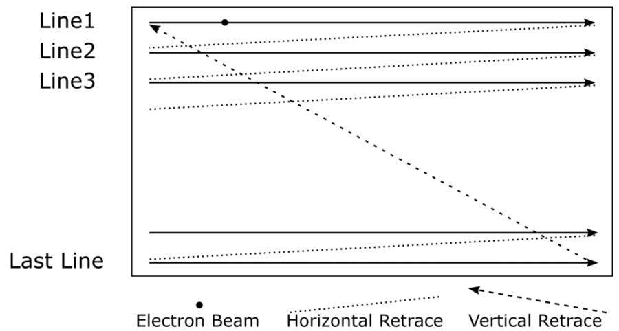
A video stream is composed of a series of frames displayed at a fixed timing interval. This timing interval can be described using Frames Per Second (FPS) or Hz. The roots of this process come from the old CRT displays when an electron beam was continuously steered across the back of the screen to illuminate a picture.
This horizontal retrace is not instantaneous. A certain amount of time is required to steer the beam from the right back to the left and then to stabilize the beam before the start of the next line. This entire process is known as the horizontal blanking interval:
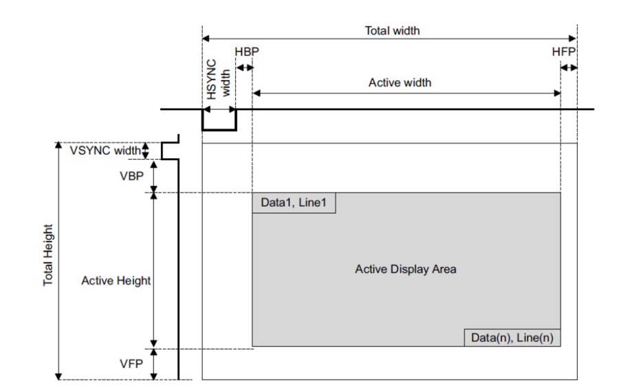
- Horizontal Front Porch (HFP): The time interval required to switch off and turn around the beam once the beam has passed the end of the display line.
- Horizontal Sync Pulse (HSYNC): The time interval required to steer the beam back across the screen.
- Horizontal Back Porch (HBP): The time interval required to stabilize the beam before it is turned on to illuminate the next line.
The vertical retrace requires a certain amount of time which is called vertical blanking:
- Vertical Front Porch (VFP): The time interval required to turn around the beam on the last line of the image is displayed.
- Vertical Sync Pulse (VSYNC): The time interval required to steer the beam from the bottom to the top of the screen.
- Vertical Back Porch (VBP): The time interval required to stabilize the beam vertically before starting the first line.
Modern digital displays no longer need time to steer an electron beam around but they still make use of these blanking periods for things like image processing and sending additional data (audio in the case of HDMI, or embedded image data for CSI-2).
The electron beam is a useful mental model. Pixel data is transmitted serially one after another moving left to right and top to bottom. There are gaps in this pixel data for the various blanking intervals. These blanking intervals are what define the image width and position relative to the display.
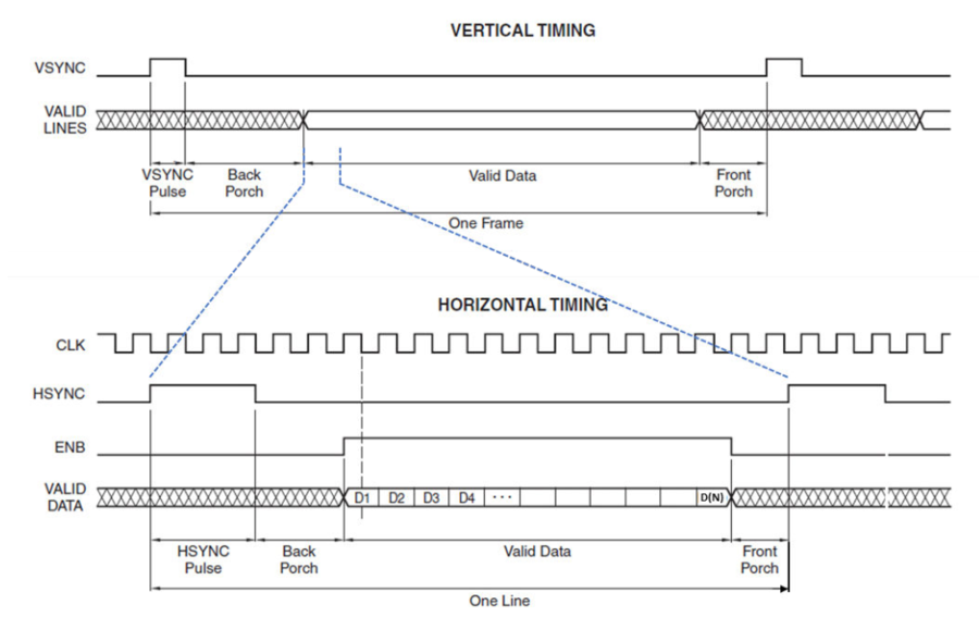
A single horizontal line of image data is signaled by the assertion of an HSYNC pulse. That pulse is followed by the HBP, then the active pixel data, and finally the HFP. The HSYNC pulse, HBP, and HFP all use pixels for their unit of measurement.
A VSYNC pulse signals the start of a new frame. That pulse is followed by the VBP then the active image lines and finally the VFP. This process repeats for the next image frame. The VSYNC, VBP, and VFP all use horizontal image lines as their unit of measurement.
To sum up the previous information, even though the electron beam is no longer used by modern displays and image systems, the blanking intervals and pulse signals are kept for synchronization purposes when transmitting the serial data bytes, and also it helps to determine the active pixel's width and height of an image.
Vertical and Horizontal Timing (Pixel Clock)
A clock must keep the pixel data and synchronization signals in order. This clock is known as a Pixel clock. A single pixel is transferred every clock cycle. It is the primary clock for most image display transport systems. In the case of Image Sensors, the pixel clock time period sets the time interval for the ADC conversion of each pixel. It is the root clock for HSYNC and VSYNC signals. HSYNC signals the start of each line and VSYNC signals the start of each new frame.
The ENB signal is used to signal active pixel data transfers. Without it, the various pixel pipelines could mistake blanking data as pixel data with a 0 value.
CSI-2 Video Timing
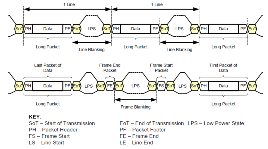
The CSI-2 low-level protocol turns the pixel data, VSYNC, and HSYNC pulses into a series of packets. The packets are sent over the physical D-PHY interface while maintaining the critical timing parameters related to each other.
The VSYNC signal is communicated using a frame start (FS) packet. The HSYNC signal is communicated using a Line Start (LS) packet.
Packet Details
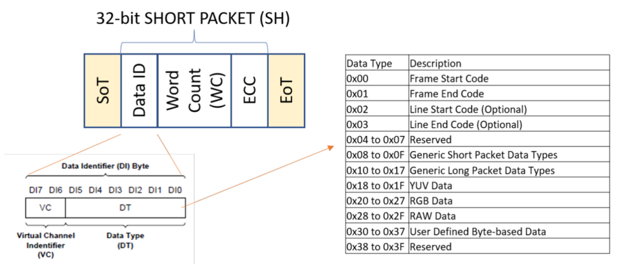
After a Start of Transmission (SOT) process, a short packet is sent. It tells the receiver what to expect next, sync signals, data, virtual channel info, or user-defined data.
Pixel/Byte Packing
Old image sensors (pre-dating the CSI-2 standard) use a parallel bus to output the ADC data to a SOC or dedicated image processor. For instance, a 10-bit wide data bus plus line, frame, and clock signals are at a minimum of 13 signals wide. A flash or other functions requires additional pins. The CSI-2 hardware block in the transmitter takes the image data from the parallel bus and packs it into a serial byte stream which can be transmitted over a DPHY Lane.
The CSI-2 standard supports various pixel formats and bit lengths. The RAW8 pixel/byte packing example is the simplest and easiest format to understand of all the various image data standards covered by CSI-2 because each data byte contains the value of a single pixel.
The RAW10 format from the OV5640 has a 10-bit pixel value but the CSI-2 standard specifies that the minimum data width is 1 byte. Since it's not possible to transfer partial pixel data, the CSI-2 has various pixel packing standards based on the pixel format used. The transmission of 10-bit RAW pixel data is done by packing four 10-bit pixel values across 5 bytes (5 * 8 bits (1 byte) = 40 bits). The minimum data packet length in this case is always 5 bytes. The standard takes as a base the bits per pixel value and looks for a value that has to be a multiple of 1 byte (8 bits). If the line to be translated does not have a pixel width evenly divisible by five, the extra pixels are zero-padded. The following table shows the CSI-2 supported formats packet data size constraints.
| Data format | Bits per Pixel (bpp) | Pixels per packet (min) | Packet length (byte) |
|---|---|---|---|
| YUV420 8-bit (legacy) | 12 | 2 | 3 |
| YUV420 8-bit | 12 | 2 | 2/4 |
| YUV420 10-bit | 15 | 4 | 5/10 |
| YUV422 8-bit | 16 | 2 | 4 |
| YUV422 10-bit | 20 | 2 | 5 |
| RGB888 | 24 | 1 | 3 |
| RGB666 | 18 | 4 | 9 |
| RGB565 | 16 | 1 | 2 |
| RGB555 | 15 | 1 | 2 |
| RGB444 | 12 | 1 | 2 |
| RAW6 | 6 | 4 | 3 |
| RAW7 | 7 | 8 | 7 |
| RAW8 | 8 | 1 | 1 |
| RAW10 | 10 | 4 | 5 |
| RAW12 | 12 | 2 | 3 |
| RAW14 | 14 | 4 | 7 |
Bandwith Calculations
In order to set or evaluate an image capture system, the system bandwidth must be calculated to ensure that the various clocks support the desired system. The basis of all image system design is the Pixel Clock which can be calculated using the following equation ( this and the subsequent formulas were taken from the i.MX8 RT MIPI DSI and CSI 2 documentation):
Pixel Clock (Hz) = HTOT * VTOT * FPS
Where:
- HTOT: Total line width = active pixels + horizontal blanking (pixels)
- VTOT: Total frame height = active lines + vertical blanking (lines)
- FPS: Frames per second
The total system bandwidth is the pixel clock times the bits per pixel. It can be calculated as:
Bandwidth (bps) = Pixel Clock * Bits Per Pixel (bpp)
Remember that the sensor output format determines the bits per pixel value. The data rate per lane is the bandwidth divided by the number of data lanes in the system design. The CSI-2 allows a minimum of 1 lane and a maximum of 4 lanes.
Data Rate Per Lane (bps) = Bandwith / number of data lanes
Also the NVIDIA Sensor Driver Programming Guide (see references section), includes other options to perform the Pixel Clock calculations. Using the PLL multiplier and PLL pre/post dividers:
MCLK multiplier = PLL multiplier / PLL pre-divider / PLL post-divide
Pixel Clock (Hz) = MCLK × MCLK multiplier
Using the sensor CSI lane output rate:
Pixel Clock (Hz) = Data Rate Per Lane (Mbps) * number of data lanes / Bits Per Pixel (bpp)
Remember that this wiki shows the general concepts defined by the CSI-2 standard but is the developer's responsibility to check the specific information of the sensor involved, by reading the respective datasheets or contact directly the camera sensor's vendor.
Relevant Clocks
Master Clock
The Master Clock, often abbreviated as MCLK, is a timing signal used in camera devices to synchronize various internal operations of the camera sensor, such as pixel readout and analog-to-digital conversion.
The purpose of the MCLK signal is to provide a stable and precise timing reference for the camera sensor's internal operations. This signal is used to determine the rate at which the sensor's clock-dependent circuits operate, ensuring that they perform their functions accurately and reliably. The MCLK signal is also used to synchronize the timing of the Pixel Clock and other signals. Basically, is the signal frequency that makes the integrated circuit operate.
The source of the MCLK signal depends on the camera device's design and can vary between different cameras. In some camera systems, the MCLK signal is generated by an external clock source, such as a crystal oscillator or a clock generator. In other cases, the MCLK signal may be generated by the camera's processor or another component within the camera system.
Pixel Clock
As we've talked about in other sections of this wiki, the Pixel Clock (often abbreviated as PCLK) is a timing signal used in camera devices that determines the rate at which the sensor outputs pixel data.
The PCLK signal is used to determine the timing of the image data, including the start and end of each pixel and each line of pixels, as well as the synchronization of the timing with other signals, such as the MIPI Clock.
The source of the PCLK signal is typically the camera sensor itself. The PCLK signal is usually provided as a digital signal in parallel with the pixel data, and it can also be provided as a separate signal on a dedicated clock lane. The frequency of the PCLK signal is determined by the sensor's design and the image resolution and frame rate that the sensor is configured to output (review the previous section with the calculations formulas for the pclk). Higher-resolution images and faster frame rates require a higher frequency PCLK signal.
MIPI Clock
The MIPI Clock (also called MIPI-CSI clock or CSI-2 Clock) is a timing signal used in camera devices that use the MIPI Alliance standards, such as CSI-2. The MIPI Clock is used to control the timing of the data transfer between the camera sensor and the receiver device, such as a processor (SoC) or an image processing unit.
The source of the MIPI Clock is typically the camera sensor itself, which generates the MIPI Clock signal as a high-frequency clock signal. Also, it is usually provided on a dedicated clock lane, separate from the data lane signals, and transmitted from the camera sensor to the receiver device.
