Difference between revisions of "Getting started with TI Jacinto 7 Edge AI/Introduction/EVM Overview"
m |
|||
| Line 24: | Line 24: | ||
[[File:Emv switches3.jpg|frameless|center|600px]] | [[File:Emv switches3.jpg|frameless|center|600px]] | ||
| + | |||
| + | ==== Board Distribution ==== | ||
| + | |||
| + | For reference on where are located the main components and their description, check the following image: | ||
| + | |||
| + | [[File:J7 som components2.png|1000px|frame|center|Image taken from [https://www.ti.com/lit/ug/spruis4a/spruis4a.pdf?ts=1620938339053&ref_url=https%253A%252F%252Fwww.google.com%252F Jacinto7 DRA829/TDA4VM Evaluation Module (EVM) Users Guide (Rev. A).]]] | ||
| + | |||
| + | ==== Configuration ==== | ||
| + | |||
| + | The switches SW1, SW2 and SW3 are called configuration switches. Depending on how this switches are set, the system on module can fulfill different functions, check the next table: | ||
| + | |||
| + | <br> | ||
| + | <br> | ||
| + | {| class="wikitable" style="margin: auto; text-align:center; vertical-align:middle;" | ||
| + | |- | ||
| + | !|Switch Name | ||
| + | !|Default Condition | ||
| + | !|Signal | ||
| + | !|Operation | ||
| + | |- | ||
| + | |SW1.1 | ||
| + | |ON | ||
| + | |LPDDR4_IO_SEL | ||
| + | |Selects the I/O voltage level for LPDDR4: | ||
| + | ‘0’ (OFF) = Selects 0.6 V I/O for LPDDR4X,‘1’ (ON) = Selects 1.1 V I/O for LPDDR4 | ||
| + | |- | ||
| + | |SW1.2 | ||
| + | |OFF | ||
| + | |SEL_SOC_I2Cn | ||
| + | |MUX to select I2C Interface for PMICs: | ||
| + | ‘0’ (OFF) = PMIC I2C to SoC WKUP interface, ‘1’ (ON) = PMIC I2C to External Header (test mode only) | ||
| + | |- | ||
| + | |- | ||
| + | |SW2.1 | ||
| + | |OFF | ||
| + | |SEL_GPIO8_ALT | ||
| + | |Selection for PMIC Watchdog Timer/GPIO8: | ||
| + | ‘0’ (OFF) = PMIC watchdog timer control is set with SW2.2, ‘1’ (ON) = PMIC I/O used for GPIO8 (test point) | ||
| + | |- | ||
| + | |- | ||
| + | |SW2.2 | ||
| + | |ON | ||
| + | |LEOA_WDOG_DIS | ||
| + | |Enable/Disable selection for PMIC Watchdog Timer: | ||
| + | ‘0’ (OFF) = PMIC watchdog timer is enabled, ‘1’ (ON) = PMIC watchdog timer is disabled | ||
| + | (requires SW2.1 to be set to OFF) | ||
| + | |- | ||
| + | |- | ||
| + | |SW3.1 | ||
| + | |ON | ||
| + | |SOC_SAFETY_ERRz | ||
| + | |Option to combine SOC_SAFETY_ERRz with MCU_SAFETY_ERR and PMIC: | ||
| + | ‘0’ (OFF) = SOC_SAFETY_ERRz (Main) is isolated from PMIC, ‘1’ (ON) = SOC_SAFETY_ERRz (Main) is connected to PMIC | ||
| + | |- | ||
| + | |- | ||
| + | |SW3.2 | ||
| + | |OFF | ||
| + | |SOC_PWR_EN | ||
| + | |Manual method of enabling PMIC: | ||
| + | ‘0’ (OFF) = PMIC enabled by EVM system, ‘1’ (ON) = PMIC enabled manually (test mode only) | ||
| + | |- | ||
| + | !colspan="4"|Note: This table is a simple rework from J721E SOM configuration switches table, located in [https://www.ti.com/lit/ug/spruis4a/spruis4a.pdf?ts=1620938339053&ref_url=https%253A%252F%252Fwww.google.com%252F Jacinto7 DRA829/TDA4VM Evaluation Module (EVM) Users Guide (Rev. A).] | ||
| + | |} | ||
<noinclude> | <noinclude> | ||
{{Getting started with TI Jacinto 7 Edge AI/Foot|Introduction/SoM_Overview|Introduction/Getting Started}} | {{Getting started with TI Jacinto 7 Edge AI/Foot|Introduction/SoM_Overview|Introduction/Getting Started}} | ||
</noinclude> | </noinclude> | ||
Revision as of 12:46, 25 June 2021
Getting started with TI Jacinto 7 Edge AI RidgeRun documentation is currently under development. |
| Getting started with TI Jacinto 7 Edge AI | ||||||
|---|---|---|---|---|---|---|
  | ||||||
| Introduction | ||||||
|
|
||||||
| GStreamer | ||||||
|
|
||||||
| Demos | ||||||
|
||||||
| Reference Documentation | ||||||
| Contact Us |
Contents
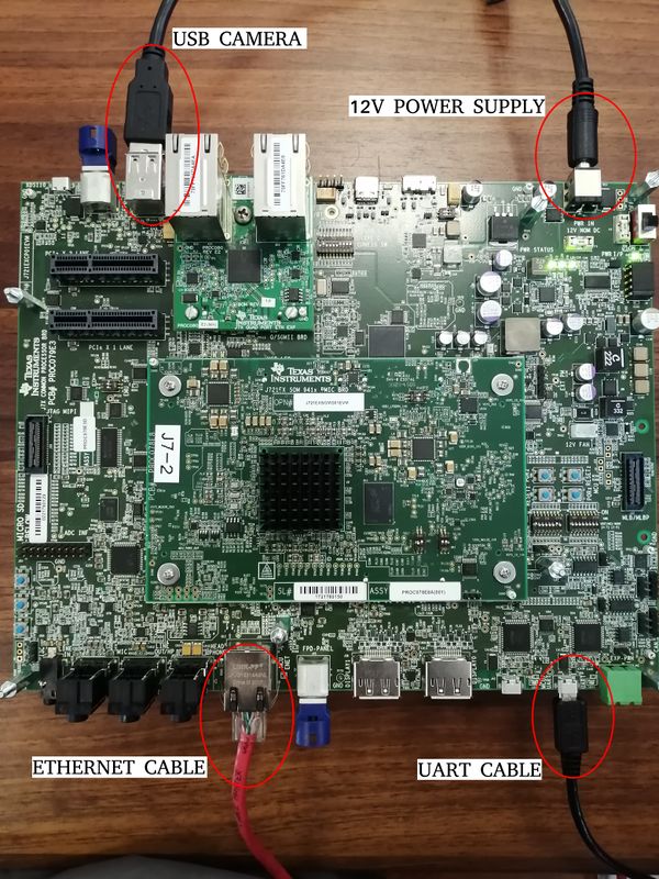
The EVM setup
Requirements:
- TDA4VM/J7ES EVM
- 12 V power supply
- Ethernet cable
- UART cable
- Minimum 16GB high-performance SD card
- USB camera
- Full HD eDP display
The EVM connections
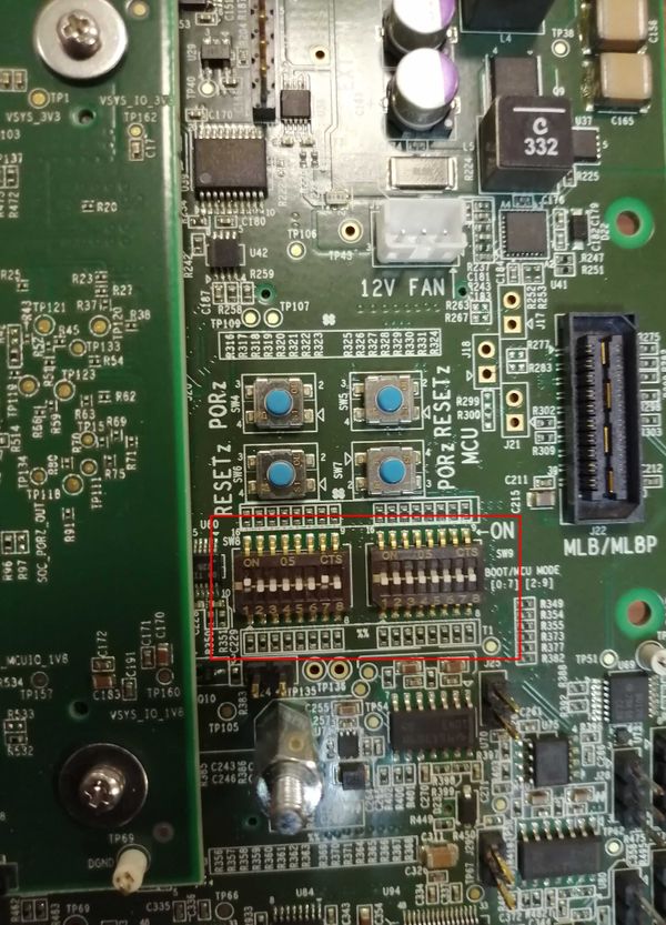
Boot mode switches
In order to allow the EVM to boot, please follow this switches configuration:
Board Distribution
For reference on where are located the main components and their description, check the following image:
Configuration
The switches SW1, SW2 and SW3 are called configuration switches. Depending on how this switches are set, the system on module can fulfill different functions, check the next table:
| Switch Name | Default Condition | Signal | Operation |
|---|---|---|---|
| SW1.1 | ON | LPDDR4_IO_SEL | Selects the I/O voltage level for LPDDR4:
‘0’ (OFF) = Selects 0.6 V I/O for LPDDR4X,‘1’ (ON) = Selects 1.1 V I/O for LPDDR4 |
| SW1.2 | OFF | SEL_SOC_I2Cn | MUX to select I2C Interface for PMICs:
‘0’ (OFF) = PMIC I2C to SoC WKUP interface, ‘1’ (ON) = PMIC I2C to External Header (test mode only) |
| SW2.1 | OFF | SEL_GPIO8_ALT | Selection for PMIC Watchdog Timer/GPIO8:
‘0’ (OFF) = PMIC watchdog timer control is set with SW2.2, ‘1’ (ON) = PMIC I/O used for GPIO8 (test point) |
| SW2.2 | ON | LEOA_WDOG_DIS | Enable/Disable selection for PMIC Watchdog Timer:
‘0’ (OFF) = PMIC watchdog timer is enabled, ‘1’ (ON) = PMIC watchdog timer is disabled (requires SW2.1 to be set to OFF) |
| SW3.1 | ON | SOC_SAFETY_ERRz | Option to combine SOC_SAFETY_ERRz with MCU_SAFETY_ERR and PMIC:
‘0’ (OFF) = SOC_SAFETY_ERRz (Main) is isolated from PMIC, ‘1’ (ON) = SOC_SAFETY_ERRz (Main) is connected to PMIC |
| SW3.2 | OFF | SOC_PWR_EN | Manual method of enabling PMIC:
‘0’ (OFF) = PMIC enabled by EVM system, ‘1’ (ON) = PMIC enabled manually (test mode only) |
| Note: This table is a simple rework from J721E SOM configuration switches table, located in Jacinto7 DRA829/TDA4VM Evaluation Module (EVM) Users Guide (Rev. A). | |||


